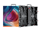
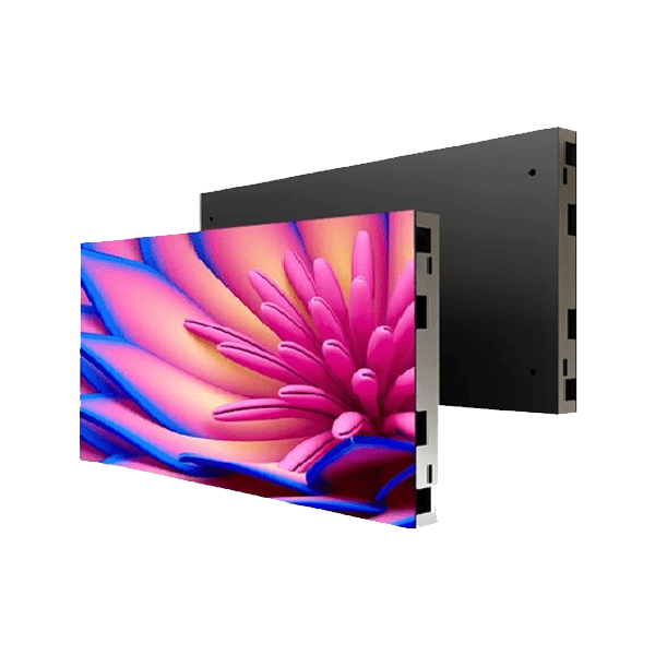
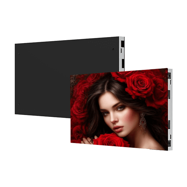
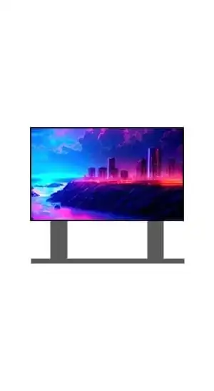
Micro LED screen displays are at the forefront of display technology, offering exceptional image quality, energy efficiency, and design flexibility. Utilizing micro LEDs, these advanced screens deliver vivid visuals with outstanding brightness and color accuracy, making them an ideal choice for home theaters and professional video display applications.
Explore the COB LED Display Screen for outstanding image quality and eco-friendly technology. Upgrade your display experience today.
Understanding MIP LED Screen (MicroLED In Package) MIP LED display screen, short for “MicroLED in Package,” is an advanced diode packaging technology that combines RGB diodes smaller than 100 microns into a surface mounted diode (SMD). MIP LED display screen technology demonstrates superior suitability for micro-scale chips, offering greater potential for pixel pitch reduction and […]
Micro LED displays feature breakthrough technology that delivers ultra-high brightness, fine image quality, and energy efficiency. Widely used in high-end commercial displays, command centers, and virtual production, Micro LED is recognized as the future direction of display technology.
Micro LED displays offer extremely high brightness levels, making them ideal for both indoor and outdoor use. Even under direct sunlight, visuals remain sharp and clearly visible.
With pixel-level light control and true black capability, Micro LED delivers exceptional contrast, enhancing depth and clarity for vivid and lifelike images.
Micro LED supports an ultra-wide color gamut, accurately reproducing a broader range of colors, ideal for professional applications like virtual production and broadcasting.
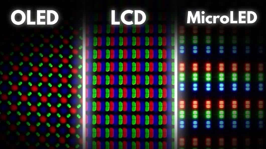
Each pixel in a Micro LED screen emits its own light, resulting in better contrast, faster response times, and superior image quality without needing a backlight.
Micro LED displays feature breakthrough technology that delivers ultra-high brightness, fine image quality, and energy efficiency. Widely used in high-end commercial displays, command centers, and virtual production, Micro LED is recognized as the future direction of display technology.
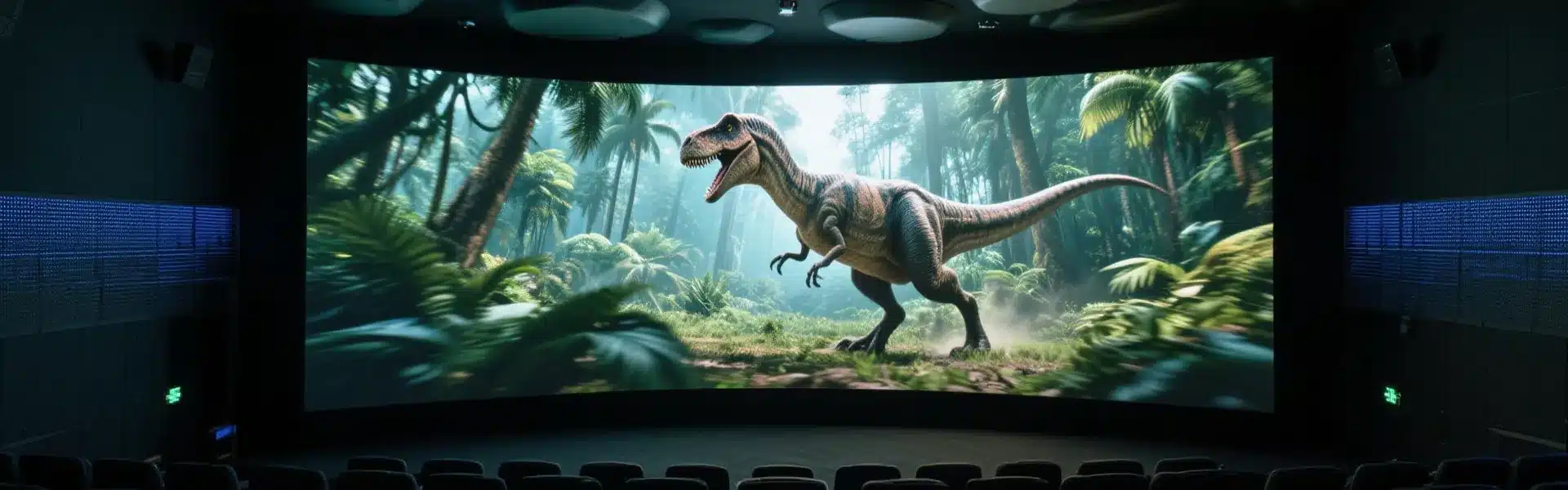
The 163-inch display delivers true native 8K resolution — no upscaling, no interpolation. Movies, TV, and documentaries play at exactly 1:1 pixel accuracy, preserving every detail and shadow exactly as intended.
Automatically adapts to the 23Hz~240Hz range, delivering smooth, cinematic playback with Netflix, Disney+, and UHD 4K 8K Blu-ray at true frame rates.
4K HDR with Dolby Vision and Atmos — stable, smooth, and cinema-ready.
Richer, truer colors — matched to cinematic standards.
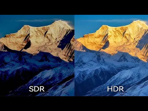
HDR10 delivers richer colors, deeper blacks, and brighter highlights — real-time scene optimization for true theater-grade picture quality at home.
22-bit+ processing unlocks 64× greater dynamic contrast and 0.001-nit brightness precision — delivering rich, accurate detail even in the darkest scenes.
Detailed technical specifications such as pixel pitch, brightness, refresh rate, and panel size help users make informed decisions based on real performance data.
| Pixel Pitch (mm) | 0.9 | 1.25 | 1.56 | 1.95 |
| Operating Environment | Indoor | Indoor | Indoor | Outdoor |
| Module Size (mm) | 150*168.75 | 150*168.75 | 150*168.75 | 250*250 |
| Cabinet Size (mm) | 600*337.5*45 | 600*337.5*45 | 600*337.5*45 | 500*500*78 |
| Cabinet Resolution (W×H) | 640*360 | 480*270 | 384*216 | 256*256 |
| IP Grade | Front IP44Rear IP54 | Front IP44 Rear IP54 | Front IP44 Rear IP54 | Front IP67 Rear IP67 |
| Weight (kg/cabinet) | 5.0 | 5.2 | 5.5 | 7.5 |
| White Balance Brightness (nit) | 600-800 | 600-1000 | 800-1200 | 4000-4500 |
| Horizontal / Vertical Viewing Angle | 160/160 | 160/160 | 160/160 | 160/160 |
| Power Consumption(W/㎡) | 250±15%/120±15% | 250±15%/150±15% | 300±15%/150±15% | 350±15%/150±15% |
| Refresh Rate(Hz) | ≥7680 | ≥7680 | ≥7680 | ≥7680 |
| Control System | Nova | Nova | Nova | Nova |
| Certification | CE, FCC, ETL | CE, FCC, ETL | CE, FCC, ETL | CE, FCC, ETL |
Micro LED displays feature breakthrough technology that delivers ultra-high brightness, fine image quality, and energy efficiency. Widely used in high-end commercial displays, command centers, and virtual production, Micro LED is recognized as the future direction of display technology.

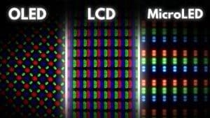
Micro LED displays offer significant advantages over traditional technologies such as LCD, OLED, and mini LED. With superior brightness, energy efficiency, and durability, micro LED stands out as a next-generation display solution for both indoor and outdoor applications. The following comparison highlights the key benefits of micro LED, helping users understand its position at the forefront of display technology.
| Feature | Micro LED | OLED | Mini LED | LCD |
|---|---|---|---|---|
| Brightness | Ultra-high (1000+ nits) | Moderate to high | High | Moderate |
| Contrast Ratio | Infinite (self-emissive) | Infinite (self-emissive) | High (with local dimming) | Low to moderate |
| Color Gamut | Wide (Rec.2020 capable) | Wide (DCI-P3) | Wide (depends on backlight) | Limited |
| Black Level | True black | True black | Good, not perfect | Washed-out blacks |
| Power Efficiency | High | Moderate | Moderate | Low |
| Lifespan | 100,000+ hours | 30,000–50,000 hours | ~50,000 hours | ~30,000 hours |
| Burn-in Risk | None | Yes | Low | None |
| Thickness | Ultra-thin | Thin | Thicker | Thick |
| Scalability | Seamless, modular | Limited | Good | Good |
| Price | High (currently) | High | Mid to high | Low |
Discover essential tips for choosing the perfect indoor LED display for your needs, ensuring efficiency and quality in installation.
while both LED walls and LED video walls offer cutting-edge visual technology, the key differences lie in their construction.
How to install indoor LED display screen To install an indoor LED display screen, follow these steps - 1. Determine…
Installing indoor LED display screens on the wall requires careful planning and execution. Here are the general steps to follow for a successful installation.
If you are interested in our products, please contact us promptly
Contact a sales expert
Stay connected with us to discover the latest innovations, exclusive offers, and insights that will elevate your business to the next level.