Revolutionizing Micro LED Screens: How SiMiP Solves Mass Transfer Challenges
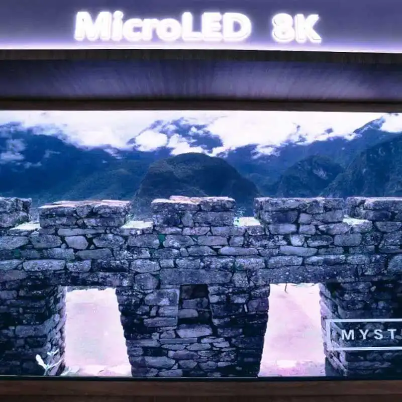
The global display industry is witnessing a paradigm shift as HKC and Lighent Semiconductor debut the world’s first silicon-based GaN monolithic integrated Micro LED screen (SiMiP). This innovation addresses the critical bottlenecks of traditional manufacturing—high costs, low yields, and environmental concerns—positioning micro-pitch LED displays (sub-P1.0) for mass adoption in commercial and consumer markets.
1. SiMiP vs. Traditional Micro LED Screens: Key Innovations
1.1 Eliminating Mass Transfer Complexity
Traditional Micro LED screens require transferring millions of RGB subpixels (1–10µm) onto driver backplanes via error-prone “mass transfer” processes. Industry yields stagnate below 70% due to alignment precision demands.
SiMiP’s breakthrough lies in its GaN-on-Si monolithic design:
- Single-Chip RGB Integration: Combines blue Micro LEDs with quantum dot (QD) color conversion layers to emit red/green light, bypassing separate chip transfers.
- 3x Faster Assembly: Reduces placement steps from 3 to 1 per pixel.
- 99.9% Pick-and-Place Yield: Leverages mature SMT equipment instead of specialized transfer tools ($1M+/unit).
1.2 Quantum Dot Color Conversion Advantages
- Zero Arsenic Materials: Replaces toxic AlInGaP red LEDs with eco-friendly InGaN blue LEDs + QD layers (EU RoHS compliant).
- Color Stability: Locks wavelengths at 630nm (red) and 530nm (green) regardless of current/temperature fluctuations (ΔE <1.5 vs. industry ΔE <3).
2. Cost and Performance Benefits for Micro LED Screens
2.1 40% Lower Packaging Costs via Wafer-Level Integration
SiMiP embeds packaging structures during GaN-on-Si wafer processing:
- Direct Chip Placement: Eliminates post-fabrication encapsulation steps.
- Material Savings: Reduces epoxy resins and phosphors by 60%.
2.2 Thermal Management Breakthroughs
- 30% Improved Heat Dissipation: GaN-on-Si substrates outperform traditional sapphire, extending lifespan to 100,000+ hours.
- Uniform Brightness: Maintains <5% luminance variance across 4K panels.
2.3 Scalability for P0.4-P0.9 Micro LED Screens
HKC’s production roadmap targets:
- 2024: 6.67″ glass-based Micro LED prototypes (500 nits, 100% NTSC).
- 2025: 5,000 monthly wafers for P0.9 commercial displays (cost: $800/㎡ vs. $2,400/㎡ traditional).
- 2026: P0.4 AR/VR screens with 5,000 PPI density.
3. Market Impact: Reshaping the $5.8B Micro-Pitch Display Sector
3.1 Disrupting COB and SMD Technologies
SiMiP’s Micro LED-in-Package (MiP) approach outperforms rivals:
| Metric | SiMiP | COB |
|---|---|---|
| Production Yield | 95% | 70–85% |
| Pixel Pitch | P0.4–P0.9 | P0.6–P1.2 |
| Module Cost (P0.9) | $800/㎡ | $2,400/㎡ |
3.2 Accelerating Domestic Supply Chain Growth
China’s display ecosystem is leveraging SiMiP to reduce foreign dependency:
- Localized Components: 70% of QD materials and GaN drivers sourced domestically by 2025.
- Patent Leadership: Lighent’s 10,000+ GaN/GaAs patents counter Samsung/LG’s Micro LED IP.
4. Future Applications Beyond Micro LED Screens
4.1 Next-Gen AR/VR Displays
- 5,000 PPI Density: Enables retinal-level resolution for metaverse devices.
- 10,000 nits Brightness: Supports outdoor mixed-reality use cases.
4.2 Automotive and Transparent Screens
- HUDs: 150% wider color gamut vs. OLED for augmented driving.
- Energy Efficiency: 0.5W power consumption per 10k nits (50% lower than LCD).
5. Challenges and Industry Outlook
While SiMiP slashes Micro LED screen costs, hurdles remain:
- QD Lifetime: Current red QD layers degrade 15% after 20,000 hours (vs. 5% for blue LEDs).
- Driver IC Complexity: 16-bit grayscale control demands advanced 28nm CMOS backplanes.
However, HKC’s $1.5B investment and partnerships with Changhong/Mianyang governments aim to:
- Cut QD costs by 30% via nanoparticle synthesis innovations.
- Achieve 80% GaN driver localization by 2026.


